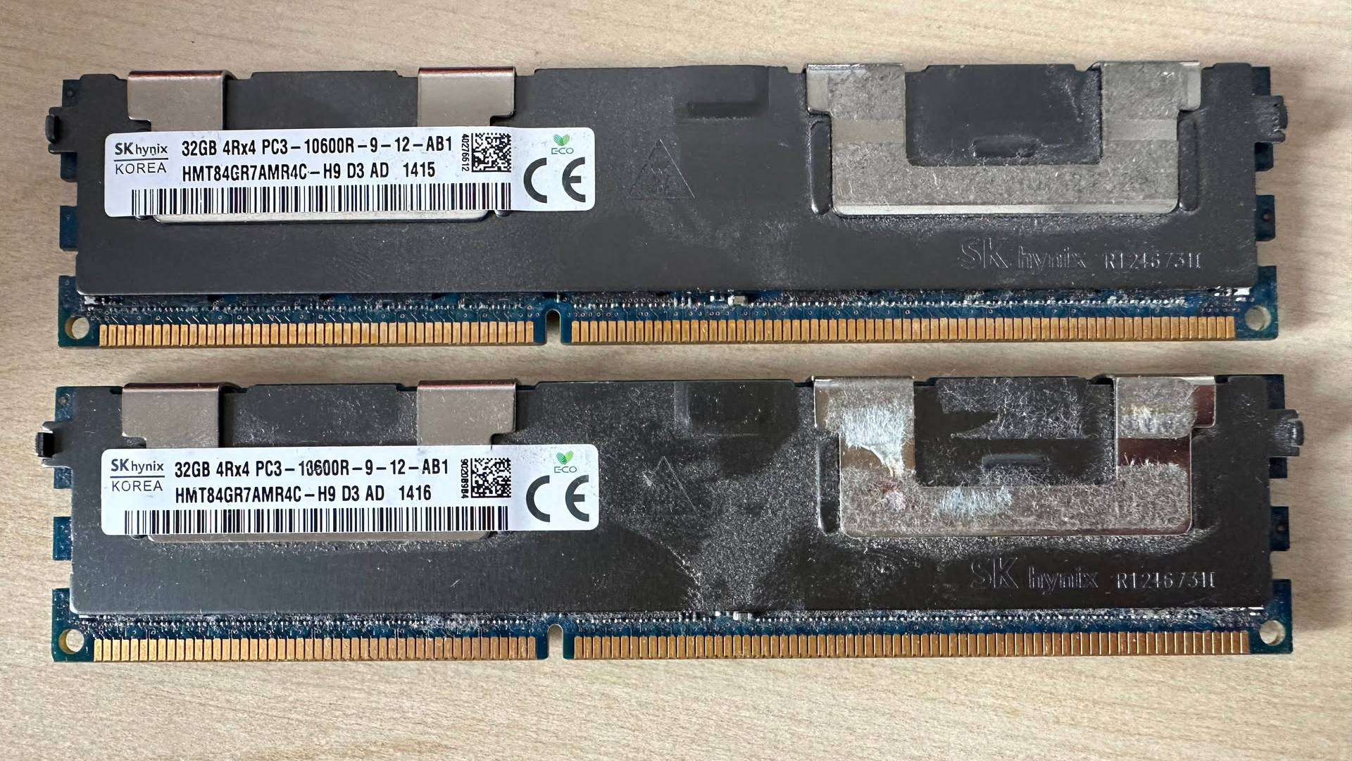
SK hynix 32 GB DDR3-1333 Registered ECC RDIMM (HMT84GR7AMR4C-H9)
•
Form Factor: 240-pin Registered DIMM (RDIMM) • Standard Height (30.0 mm PCB / 31.25 mm with Heat Spreader)
•
Standard & Density: DDR3 SDRAM • 32 GB (32,768 MB) • Quad-Rank (4Rx4)
•
Bandwidth & Timings: PC3-10600R (10.67 GB/s per channel) • CL9-9-9-24 @ 1.5V
•
Register & Telemetry: JEDEC SSTE32882 28-bit Register PLL • Integrated SPD Digital Thermal Sensor (TSE2002av)
•
Museum Inventory: 2 Physical Units (Date Codes: 1415 • 1416 • SK hynix Korea)
•
Active Host Pairing: Dell Precision T7610 Workstation (Dual NUMA Sockets • mc0/mc1 Channel 0 • 64 GB Pool)
1. Technical Overview & Key Specifications Table
| Category | Property | Specification |
|---|---|---|
| Module Identity | Manufacturer | SK hynix Inc. (Icheon / Cheongju, Republic of Korea) |
| Product Part Number | HMT84GR7AMR4C-H9 |
|
| Module Capacity | 32 GB (32,768 MBytes / 34,359,738,368 Bytes) | |
| JEDEC Raw Card Reference | PC3-10600R-9-12-AB1 (JEDEC Raw Card AB, Revision 1) |
|
| Form Factor & Pin Count | 240-pin Registered Dual In-Line Memory Module (RDIMM) | |
| Target Market Segment | Mission-Critical Enterprise Servers, High-Performance Workstations, Cloud Compute Nodes | |
| Commercial Era / Production | April 2014 (Verified Physical Date Codes: 1415 & 1416 • Weeks 15-16, 2014) | |
| DRAM Silicon & Packaging | DRAM Die Density | 4 Gb (512M × 8-bit internal bank architecture / 1G × 4-bit config) |
| DRAM Die Generation | SK hynix 30nm-class C-Die (AMR4C series stepping) | |
| Internal Bank Architecture | 8 Independent Internal Banks per DRAM Die | |
| Total DRAM Silicon Dies | 72 Silicon Dies (18 dies per rank × 4 ranks) | |
| Physical Package Count | 36 Dual-Die Packages (DDP) / 78-ball Fine-pitch Ball Grid Array (FBGA) | |
| Package Layout on PCB | 18 DDP FBGA packages on Front Side, 18 DDP FBGA packages on Back Side | |
| Rank Organization | Quad-Rank (4Rx4) • 4 physical chip-select ranks (CS0_n, CS1_n, CS2_n, CS3_n) | |
| Device Data Width | x4 bit-slice organization per DRAM component (72-bit ECC bus width) | |
| Timings & Clock Profiles | JEDEC Speed Bin | DDR3-1333 (JEDEC standard PC3-10600) |
| Data Transfer Rate | 1,333 MT/s (Mega-transfers per second per data pin) | |
| I/O Bus Clock Frequency | 667 MHz (Double Data Rate: 2 transfers per clock cycle) | |
| Internal Memory Core Clock | 166.67 MHz (8n Prefetch Architecture) | |
| CAS Latency (CL) | 9 Clock Cycles (13.50 ns absolute access time) | |
| Primary JEDEC Timings | 9-9-9-24 (CL: 9 • tRCD: 9 • tRP: 9 • tRAS: 24) | |
| Row Cycle Time (tRC) | 49.50 ns (33 clock cycles) | |
| Peak Module Bandwidth | 10,667 MB/s (10.67 GB/s) per single memory channel | |
| Register, Buffer & Telemetry | Register PLL Silicon | JEDEC SSTE32882 Compliant 28-bit 1:2 Register Buffer with Phase-Locked Loop |
| Address & Control Buffering | Fully registered and re-clocked address, command, and control signals | |
| Clock Distribution | Differential clock input (CK, CK#) phase-locked and re-driven to all 36 DRAM packages | |
| SPD EEPROM & Sensor | 256-Byte Serial Presence Detect with integrated TSE2002av digital thermal sensor | |
| Thermal Sensor Accuracy | ±0.5°C typical (±1.0°C max across -20°C to +100°C range via I2C/SMBus) | |
| Electrical & Power | Supply Voltage (VDD / VDDQ) | 1.5V ± 0.075V standard DDR3 operating voltage |
| I/O Signaling Standard | SSTL_15 (Stub Series Terminated Logic 1.5V) with dynamic On-Die Termination (ODT) | |
| Termination Voltage (VTT) | 0.50 × VDD (0.75V nominal) tracking power plane | |
| Reference Voltage (VREF) | 0.50 × VDD (0.75V) for address, command, and data lines | |
| Typical Module Power Draw | ~7.5W to 9.2W under full-span active write/read bursts; ~2.1W idle | |
| Refresh Dynamics | Auto-Refresh (tRFC: 260 ns) • Average Periodic Interval (tREFI: 7.8 μs at ≤85°C, 3.9 μs at >85°C) | |
| Physical, Mechanical & Thermal | Module Dimensions | 133.35 mm (L) × 30.00 mm (PCB Height) × ~7.50 mm (Thickness with Spreader) |
| PCB Substrate | 8-layer high-frequency low-loss FR-4 with gold-plated contact fingers | |
| Edge Contact Plating | Hard Gold Plating (minimum 30 μ-inch gold over 50 μ-inch nickel) | |
| Heat Spreader Construction | Factory-installed stamped full-coverage dark anodized aluminum heat spreader | |
| Heat Spreader Stamping | SK hynix R124673H (Permanent metal stamp on lower right face) |
|
| Retention Clips | Dual heavy-gauge spring steel top retention clips providing continuous thermal pad pressure | |
| Reliability & ECC Protection | Data Bus Width | 72-bit (64 data bits + 8 ECC syndrome parity check bits) |
| Error Correction Capability | Single-Bit Error Correction (SEC), Double-Bit Error Detection (DED) via Hamming syndrome | |
| Chipkill / SDDC Readiness | Fully qualified for Single Device Data Correction (SDDC / Chipkill) due to x4 DRAM organization | |
| Memory Scrubbing Engine | Supports background patrol scrubbing and demand scrubbing on Intel C602 / Romley platforms | |
| Host Platform Compatibility | Intel Xeon E5-2600 v1/v2, Xeon E5-4600 v1/v2, Xeon E7 v2, AMD Opteron 6300 G34 server systems | |
| Museum Hardware Provenance | 2 Verified Units deployed in Dell Precision T7610 Workstation (Exhibit #2973) |
2. Memory Rank Architecture & Quad-Rank Subsystem Dynamics
Achieving a staggering 32 GB module capacity within the electrical and physical constraints of the DDR3 generation was an extraordinary engineering triumph. Because standard DDR3 DRAM dies topped out at 4 Gb (Gigabits) per discrete chip, creating a 32 GB (256 Gigabit) module required assembling exactly 72 discrete DRAM dies onto a single 240-pin PCB substrate.
Quad-Rank (4Rx4) Organization
The module is segmented into four independent electrical ranks (Rank 0 through Rank 3). Each rank consists of 18 x4 DRAM devices (16 devices yielding the 64-bit primary data word, plus 2 devices providing the 8-bit ECC syndrome check bits). The host memory controller selects active ranks via four dedicated chip-select lines (CS0_n, CS1_n, CS2_n, CS3_n).
Dual-Die Package (DDP) Stacking
Because a standard 240-pin DIMM PCB can physically fit at most 36 discrete FBGA packages across both faces, SK hynix deployed Dual-Die Package (DDP) wire-bonding technology. Each 78-ball FBGA package houses two stacked 4 Gb C-die silicon slices connected to shared address and data buses with separate chip-enable pads, condensing 72 silicon dies into 36 physical surface-mount components.
Register Buffer & Bus Loading
Driving 72 DRAM devices directly from a CPU memory controller would induce catastrophic capacitive loading, degrading high-speed signal integrity. The central JEDEC SSTE32882 register/PLL IC intercepts all command, address, and control lines, re-driving them cleanly across the board so that the host controller sees only a single electrical load per module for these critical signal lines.
Platform Population Considerations: Because Quad-Rank modules present four rank loads to the memory controller’s chip-select arbitration logic, enterprise platforms such as Intel Romley (Xeon E5-2600) restrict DIMMs-per-channel (DPC) population rules when 4R RDIMMs are used. In a 3-slot-per-channel motherboard, populating a Quad-Rank RDIMM typically limits the channel to a maximum of two populated slots and automatically clocks the bus at 1066 MT/s or 1333 MT/s. In contrast, 1 DPC configurations easily sustain full DDR3-1333 MT/s operation at CL9.
3. Monospace ASCII Silicon Architecture & Pinout Bus Schematic
The following architectural schematic illustrates the complete signal flow, clock distribution, registered command buffering, and 4-rank DRAM topology of the SK hynix HMT84GR7AMR4C-H9 module:
+-----------------------------------------------------------------------------------------------------------------------+
|                       SK HYNIX HMT84GR7AMR4C-H9 ARCHITECTURE (32 GB 4Rx4 PC3-10600R RDIMM)                             |
|                                                                                                                       |
|  [ HOST INTEGRATED MEMORY CONTROLLER (LGA 2011 IMC / INTEL XEON E5-2600 v1/v2) ]                                     |
|     |                                                                                                                 |
|     +== 64-bit Bidirectional Data Bus (DQ0 - DQ63) ==============================================+                   |
|     +== 8-bit ECC Syndrome Bus (CB0 - CB7) ===================================================+  |                   |
|     |                                                                                         |  |                   |
|     +-- Command/Address/Control Bus (A0-A15, BA0-BA2, RAS#, CAS#, WE#, ODT, CKE)              |  |                   |
|     +-- Differential Host Clock Pair (CLK_t / CLK_c)                                          |  |                   |
|     +-- I2C / SMBus Serial Management (SCL, SDA, EVENT#)                                      |  |                   |
|     |                                                                                         |  |                   |
|  [ 240-PIN EDGE CONNECTOR (RAW CARD AB1 / GOLD PLATED FINGERS) ]                             |  |                   |
|     |                                                                                         |  |                   |
|     +---> [ I2C / SMBus ] ---> [ 256-BYTE SPD EEPROM + TSE2002av DIGITAL THERMAL SENSOR ]     |  |                   |
|     |                                                                                         |  |                   |
|     +---> [ COMMAND & CLOCK ]                                                                 |  |                   |
|             |                                                                                 |  |                   |
|             v                                                                                 |  |                   |
|     +-----------------------------------------------------------------------------------+     |  |                   |
|     |          JEDEC SSTE32882 28-BIT 1:2 REGISTER BUFFER & PHASE-LOCKED LOOP (PLL)     |     |  |                   |
|     |  - Differential Clock Input Regeneration & Phase Alignment (PLL Clock Output)     |     |  |                   |
|     |  - Input Command / Address Parity Checking Engine (PAR_IN -> PERR# Telemetry)     |     |  |                   |
|     |  - Re-Driven Dual Outputs: Address/Bank (Y0A/Y0B), RAS#/CAS#/WE#, ODT/CKE Drive   |     |  |                   |
|     +-----------------------------------------------------------------------------------+     |  |                   |
|             |                       |                       |                       |         |  |                   |
|             | (Buffered Addr/Cmd)   | (Buffered Addr/Cmd)   | (Buffered Addr/Cmd)   |         |  |                   |
|             v                       v                       v                       v         v  v                   |
|     +---------------+       +---------------+       +---------------+       +---------------+                        |
|     |    RANK 0     |       |    RANK 1     |       |    RANK 2     |       |    RANK 3     |                        |
|     |   (CS0_n)     |       |   (CS1_n)     |       |   (CS2_n)     |       |   (CS3_n)     |                        |
|     | 18x 4Gb Dies  |       | 18x 4Gb Dies  |       | 18x 4Gb Dies  |       | 18x 4Gb Dies  |                        |
|     | (16 Data +    |       | (16 Data +    |       | (16 Data +    |       | (16 Data +    |                        |
|     |   2 ECC x4)   |       |   2 ECC x4)   |       |   2 ECC x4)   |       |   2 ECC x4)   |                        |
|     +---------------+       +---------------+       +---------------+       +---------------+                        |
|             |                       |                       |                       |                                |
|             +-----------------------+-----------------------+-----------------------+                                |
|                                                 |                                                                    |
|                       72-bit Memory Slice (64-bit Data + 8-bit ECC)                                                  |
|                             36x Dual-Die Packages (DDP) FBGA-78                                                      |
|               Covered by Factory SK hynix R124673H Full-Coverage Aluminum Heat Spreader                              |
+-----------------------------------------------------------------------------------------------------------------------+
4. DRAM Cell Dynamics, Refresh Physics & Power Management
At the silicon microscopic level, each bit of the 34.36 billion bytes packed into this module is stored within a microscopic 1T-1C (one transistor, one capacitor) memory cell fabricated using SK hynix’s 30nm-class process. Due to sub-micron quantum tunneling and dielectric leakage, the microscopic charge stored across each cell capacitor naturally drains over time, mandating precise refresh timing:
Refresh Timing (tREFI & tRFC)
All 8,192 row addresses must be refreshed every 64 ms under standard operating temperatures (≤85°C), demanding an average periodic refresh interval (tREFI) of 7.8 μs. For 4 Gb density dies, each row refresh cycle (tRFC) requires 260 ns of memory bus occupation. When the integrated thermal sensor detects junction temperatures exceeding 85°C, Auto-Self-Refresh (ASR) doubles the refresh rate (tREFI = 3.9 μs) to preserve data retention.
SSTL_15 Signaling & Dynamic ODT
High-frequency data transfer across the 240-pin edge interface utilizes Stub Series Terminated Logic (SSTL_15) at 1.5V. To prevent transmission line signal reflections across four ranks, each DRAM die incorporates programmable On-Die Termination (ODT). The memory controller dynamically switches termination resistance (RTT_Nom: 60Ω/40Ω; RTT_WR: 120Ω) between active read and write operations.
Thermal Engineering (R124673H)
Operating 72 DRAM dies and a high-power register buffer generates substantial heat (~8-9W under peak load). Uncooled 4Rx4 modules would easily exceed 95°C in server chassis without extreme airflow. SK hynix mitigated this by enclosing the module in a factory-installed stamped aluminum heat spreader (Part: R124673H) clamped with high-tension spring steel clips, dissipating thermal energy evenly across the entire surface.
5. Enterprise Data Integrity: Single-Bit Correction & Multi-Bit Detection
In enterprise mission-critical environments, cosmic ray alpha particles and thermal flux can randomly flip capacitor charges (soft errors). The HMT84GR7AMR4C-H9 implements a multi-tiered data protection hierarchy:
| Integrity Feature | Hardware Mechanism | Operational Benefit |
|---|---|---|
| SECDED ECC (72-bit Bus) | 8-bit Hamming Syndrome check bits appended to every 64-bit data word | Detects and automatically corrects 100% of single-bit errors in hardware; detects 100% of double-bit errors to prevent silent data corruption (SDC). |
| x4 Chipkill / SDDC | x4 device organization distributes each 4-bit nibble across different DRAM packages | Enables Single Device Data Correction (SDDC / Chipkill) on Intel Xeon E5-2600 platforms. If an entire DRAM chip suffers physical silicon failure, the system reconstructs the missing 4 bits and continues operation without downtime. |
| Register Command Parity | JEDEC SSTE32882 register calculates parity across address and command pins | If a bus transmission error occurs on address/control lines, the register flags PERR# to the host memory controller, preventing spurious write commands to wrong memory addresses. |
| Hardware Patrol Scrubbing | Autonomous background memory controller read-verify-rewrite cycles | Scans entire 32 GB address space periodically (e.g. every 24 hours), correcting single-bit soft errors in DRAM cells before a second bit flip can occur in the same word. |
| Onboard Thermal Telemetry | Integrated JEDEC TSE2002av digital temperature sensor on SPD bus | Provides real-time module temperatures to host BMC / BIOS via SMBus, triggering closed-loop server fan speed adjustments or memory clock throttling if thresholds are breached. |
6. Multi-Channel Bandwidth Scaling & Latency Profiles
When installed in enterprise server platforms like the Intel Xeon E5-2600 v1/v2 family (Socket R / LGA 2011), the integrated quad-channel memory controller interleaves access across multiple memory channels:
| Configuration Mode | Active Bus Width | Theoretical Bandwidth | Platform Application |
|---|---|---|---|
| Single-Channel (1 DIMM) | 64-bit (+8-bit ECC) | 10.67 GB/s (10,667 MB/s) | Diagnostic / Baseline single-slot boot mode |
| Dual-Channel (2 DIMMs) | 128-bit (+16-bit ECC) | 21.33 GB/s (21,333 MB/s) | Populated in 2 channels per socket (e.g. Dell T7610 baseline) |
| Triple-Channel (3 DIMMs) | 192-bit (+24-bit ECC) | 32.00 GB/s (32,000 MB/s) | LGA 1366 legacy workstation/server architectures (X8DAH) |
| Quad-Channel (4 DIMMs) | 256-bit (+32-bit ECC) | 42.67 GB/s (42,667 MB/s) | Full saturation per socket on LGA 2011 (Romley platform) |
| Dual-Socket Quad-Channel | 512-bit Aggregate | 85.33 GB/s (85,333 MB/s) | Dual Intel Xeon E5-2600 v1/v2 NUMA system aggregate throughput |
tAA = CL × tCK = 9 × 1.50 ns = 13.50 ns.This provides exceptionally responsive random access times, rivaling higher-frequency memory that operates with looser CAS latencies (such as DDR4-2400 CL17 at 14.17 ns).
7. Curator’s Assessment & Homelab Applicability
- Museum Hardware Provenance: Mateo’s Museum collection preserves 2 authentic physical units of the SK hynix 32 GB DDR3-1333 Registered ECC RDIMM (Part:
HMT84GR7AMR4C-H9). Optical inspection confirms production date codes of Week 15, 2014 (Label:1415, 2D Tag:40276612) and Week 16, 2014 (Label:1416, 2D Tag:90206984), both featuring original stamped aluminum heat spreaders (SK hynix R124673H). - Active Workstation Deployment: Both units are currently actively deployed in the museum’s primary enterprise computing workhorse, the Dell Precision T7610 Workstation (Exhibit #2973). Each module is populated into Channel 0 of the respective CPU socket (mc0 DIMM1 for CPU 1, mc1 DIMM1 for CPU 2), providing a balanced 64.0 GB dual-socket NUMA pool expandable to 512 GB across all 16 slots.
- Historical Pinnacle of DDR3 Density: The 32 GB RDIMM was the highest density per module ever achieved in standard registered DDR3 technology prior to the adoption of LRDIMMs and the transition to DDR4. Delivering 32 GB across 72 discrete silicon dies required state-of-the-art packaging and thermal management that remains an awe-inspiring example of silicon engineering.
- Homelab Virtualization Sweet Spot: In modern homelab operations, memory capacity is almost always the first resource bottleneck when deploying virtual machines on Proxmox VE, TrueNAS SCALE, or Docker containers. High-density 32 GB modules allow workstations like the T7610 to host dense ZFS ARC caches and extensive Linux containers while consuming a fraction of the available DIMM slots.
8. Authentic Hardware Photography & Physical Silicon Inspection
High-resolution physical optical inspection of the museum’s twin SK hynix 32 GB DDR3 RDIMMs, verifying manufacturing dates, lot barcodes, and stamped thermal heat spreaders:
Exhibit 8.1: Museum Artifact Label & Stamped Heat Spreader Inspection

Museum Hardware Artifact: Authentic photographic macro inspection of the museum’s two physical SK hynix 32 GB DDR3 RDIMM modules. The factory nameplate labels display the full JEDEC string 32GB 4Rx4 PC3-10600R-9-12-AB1, country of origin (KOREA), and consecutive manufacturing date codes (1415 and 1416). Visible on the lower right face of both modules is the factory metal stamping: SK hynix R124673H.
Label Markings Decoded
SK hynix: Manufacturer corporate brandmark.32GB 4Rx4: 32 Gigabytes density organized into four x4-bit electrical ranks.PC3-10600R: Standard DDR3-1333 Registered ECC DIMM specification.-9-12-AB1: CAS Latency 9, JEDEC delay bin 12, JEDEC Raw Card AB revision 1.KOREA: Country of origin (SK hynix Korea wafer fabrication and assembly).HMT84GR7AMR4C-H9: Factory part number (4Gb C-Die, DDR3-1333 speed bin).D3 AD: DRAM component stepping and internal assembly test identifier.1415/1416: Manufacturing date codes: Week 15, 2014 & Week 16, 2014.ECO / CE: European Conformity and Lead-Free / RoHS environmental compliance.
Mechanical & Thermal Engineering Details
SK hynix R124673H: Stamped heat spreader part designation on lower-right anodized surface.- Spring Steel Clips: Dual top retention brackets applying uniform mechanical pressure across thermal interface pads.
- 240-Pin Gold Fingers: Undamaged 30 micro-inch hard gold plating providing corrosion-resistant electrical coupling.
- Center Notch Alignment: Standard DDR3 keying notch located at 70.87 mm from pin 1, preventing accidental insertion into DDR2 or DDR4 sockets.
- Thermal Isolation: Protects dual-die stacked DRAM silicon and central register buffer from thermal throttling in dense 2U/4U workstation enclosures.