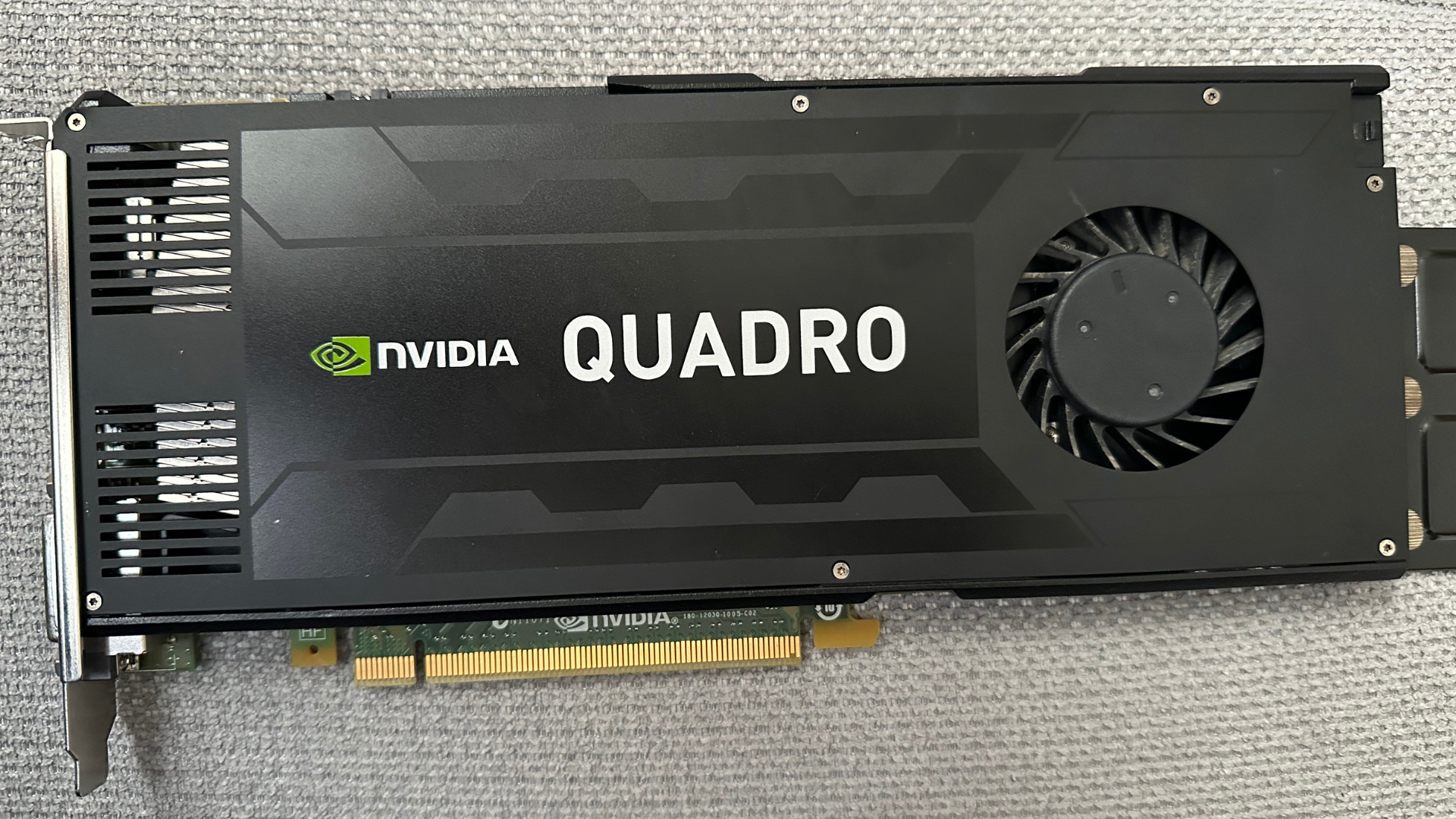
HP NVIDIA Quadro K4000 3 GB (713381-001)
Exhibit Type: Professional Workstation Graphics Accelerator & Silicon Specification Dossier
•
Microarchitecture: Kepler • GK106GL (28 nm TSMC)
•
Compute Pipeline: 768 CUDA Cores (4 SMX) • 64 TMUs • 24 ROPs • 810 MHz Core Clock
•
VRAM & Bus: 3 GB GDDR5 • 192-bit Interface • 134.4 GB/s Bandwidth • PCIe 2.0 x16
•
PassMark G3D Mark: 2,718 (Rank #7 in Museum GPU Collection)
•
Museum Inventory: 1 Physical Unit (HP Spare: 713381-001 • HP Assy: 700104-001 • S/N: 0322314010635)
•
Active Host Pairing: Dell Precision T7610 Workstation (PCIe Slot 2 • Bus 03:00.0)
•
Microarchitecture: Kepler • GK106GL (28 nm TSMC)
•
Compute Pipeline: 768 CUDA Cores (4 SMX) • 64 TMUs • 24 ROPs • 810 MHz Core Clock
•
VRAM & Bus: 3 GB GDDR5 • 192-bit Interface • 134.4 GB/s Bandwidth • PCIe 2.0 x16
•
PassMark G3D Mark: 2,718 (Rank #7 in Museum GPU Collection)
•
Museum Inventory: 1 Physical Unit (HP Spare: 713381-001 • HP Assy: 700104-001 • S/N: 0322314010635)
•
Active Host Pairing: Dell Precision T7610 Workstation (PCIe Slot 2 • Bus 03:00.0)
1. Technical Overview & Key Specifications Table
| Category | Property | Specification |
|---|---|---|
| GPU Identity | Product Name | NVIDIA Quadro K4000 (HP OEM Workstation Edition) |
| OEM Board Partner | Hewlett-Packard (HP Inc.) | |
| HP Part Numbers | HP Spare: 713381-001 • HP Assembly: 700104-001 |
|
| GPU Code Name & Revision | GK106GL (Variant GK106-ES-A1 / Revision A1) |
|
| PCI Device ID / Subsystem | PCI ID: 10de:11fa • Subsystem ID: 103c:079c |
|
| vBIOS Version | 80.06.76.00.07 (HP Factory Workstation Firmware) |
|
| Market Segment & Release | Professional CAD / DCC / CAE Workstation • March 1, 2013 | |
| Physical Silicon | Foundry & Lithography | TSMC (Taiwan Semiconductor Manufacturing Co.) • 28 nm Bulk CMOS (HP) |
| Transistor Count | 2,540 Million (2.54 Billion) transistors | |
| Die Surface Area | 221 mm² (Monolithic Die) | |
| PCB Markings & S/N | 900-52030-0300-000 L • S/N: 0322314010635 (HP S/N: CN42404748) |
|
| Form Factor | Single-Slot Standard Full-Height (9.5-inch / 241 mm length) | |
| Compute Pipeline | Microarchitecture | Kepler (SMX Generation) |
| CUDA Core Count | 768 CUDA Cores (4 SMX Units × 192 Cores/SMX) | |
| Texture Mapping Units (TMUs) | 64 TMUs (16 TMUs per SMX) | |
| Render Output Units (ROPs) | 24 ROPs (3 ROP Partitions of 8 ROPs each) | |
| GPU Core Base Clock | 810 MHz | |
| Single-Precision Compute (FP32) | 1.244 TFLOPS (1,244.2 GFLOPS) | |
| Double-Precision Compute (FP64) | 51.84 GFLOPS (1/24 FP32 Rate) | |
| Memory Subsystem | Dedicated VRAM Size | 3,072 MB (3 GB) GDDR5 |
| Memory Bus Width | 192-bit (3 x 64-bit Memory Controllers) | |
| Memory Clock Frequency | 1,404 MHz (5,616 MT/s Effective Data Rate) | |
| Peak Memory Bandwidth | 134.78 GB/s (134,784 MB/s) | |
| L2 Cache Size | 384 KB High-Speed L2 Cache (128 KB per 64-bit Controller) | |
| ECC Memory Support | Non-ECC GDDR5 (ECC reserved for Quadro K5000 / K6000 tiers) | |
| Display & Media I/O | Physical Video Outputs | 2 × DisplayPort 1.2 + 1 × Dual-Link DVI-I |
| Maximum Digital Resolution | 3840 × 2160 @ 60 Hz (DisplayPort 1.2) • 2560 × 1600 @ 60 Hz (Dual-Link DVI) | |
| Maximum Active Displays | Up to 3 Concurrent Independent Displays (or 4 via DP 1.2 Multi-Stream Transport) | |
| Hardware Video Acceleration | 1st Gen NVENC (H.264 up to 4K) • PureVideo HD VP5 (MPEG-2, VC-1, H.264) | |
| Thermal & Electrical | Thermal Design Power (TDP) | 80 Watts Maximum Power Consumption |
| Auxiliary Power Connector | 1 × 6-pin PCIe Auxiliary Power Connector | |
| Cooling Solution | Active Single-Slot Blower Fan with Copper Core Heatsink | |
| Live Operating Telemetry | +44.0 deg C Idle • 2100 RPM Fan Speed • 20.08 Watts Idle Power Draw | |
| API & Platform Support | DirectX Support | DirectX 12 (Feature Level 11_0) / Shader Model 5.0 |
| OpenGL / Vulkan | OpenGL 4.6 • Vulkan 1.2 | |
| Compute APIs | CUDA Compute Capability 3.0 • OpenCL 1.2 • DirectCompute | |
| Operating System Drivers | Linux nouveau DRM (Kernel 6.8 Verified) • NVIDIA Legacy 470.xx Driver |
2. GK106 Silicon Topology & Kepler SMX Architecture
The GK106 silicon chip powers NVIDIA’s mid-range Kepler lineup. Designed for high energy efficiency and workstation reliability, the SMX (Next-Generation Streaming Multiprocessor) architecture replaced Fermi’s high-frequency hot-clock design with an ultra-dense array of 192 FP32 ALU CUDA cores per SMX block:
+======================================================================================================================+
|                         NVIDIA GK106GL [QUADRO K4000] SILICON DIE & SMX COMPUTE TOPOLOGY                              |
+======================================================================================================================+

                          HOST INTERFACE: PCI EXPRESS 2.0 / 3.0 x16 BUS (ROOT PORT 00:02.0)
                                                    |
                                                    v
                                  +------------------------------------+
                                  | GIGA-THREAD ENGINE & HOST DISPATCH |
                                  +------------------------------------+
                                                    |
         +------------------------------------------+------------------------------------------+
         |                                                                                     |
         v                                                                                     v
+------------------------------------+                               +------------------------------------+
| GRAPHICS PROCESSING CLUSTER 0      |                               | GRAPHICS PROCESSING CLUSTER 1      |
|                                    |                               |                                    |
|  +-------------------------------+ |                               |  +-------------------------------+ |
|  | SMX BLOCK 0                   | |                               |  | SMX BLOCK 2                   | |
|  | - 192 FP32 CUDA Cores         | |                               |  | - 192 FP32 CUDA Cores         | |
|  | - 32 Special Func Units (SFU) | |                               |  | - 32 Special Func Units (SFU) | |
|  | - 32 Load/Store Units (LD/ST) | |                               |  | - 32 Load/Store Units (LD/ST) | |
|  | - 16 Texture Units (TMU)      | |                               |  | - 16 Texture Units (TMU)      | |
|  | - 64 KB L1 / Shared Memory    | |                               |  | - 64 KB L1 / Shared Memory    | |
|  | - PolyMorph Engine 2.0        | |                               |  | - PolyMorph Engine 2.0        | |
|  +-------------------------------+ |                               +-------------------------------+ |
|                                    |                               |                                    |
|  +-------------------------------+ |                               |  +-------------------------------+ |
|  | SMX BLOCK 1                   | |                               |  | SMX BLOCK 3                   | |
|  | - 192 FP32 CUDA Cores         | |                               |  | - 192 FP32 CUDA Cores         | |
|  | - 32 Special Func Units (SFU) | |                               |  | - 32 Special Func Units (SFU) | |
|  | - 32 Load/Store Units (LD/ST) | |                               |  | - 32 Load/Store Units (LD/ST) | |
|  | - 16 Texture Units (TMU)      | |                               |  | - 16 Texture Units (TMU)      | |
|  | - 64 KB L1 / Shared Memory    | |                               |  | - 64 KB L1 / Shared Memory    | |
|  | - PolyMorph Engine 2.0        | |                               |  | - PolyMorph Engine 2.0        | |
|  +-------------------------------+ |                               +-------------------------------+ |
+------------------------------------+                               +------------------------------------+
         |                                                                                     |
         +------------------------------------------+------------------------------------------+
                                                    |
                                                    v
         +------------------------------------------+------------------------------------------+
         |                                          |                                          |
         v                                          v                                          v
+-----------------------+                  +-----------------------+                  +-----------------------+
| MEMORY CONTROLLER 0   |                  | MEMORY CONTROLLER 1   |                  | MEMORY CONTROLLER 2   |
| - 64-bit GDDR5 Bus    |                  | - 64-bit GDDR5 Bus    |                  | - 64-bit GDDR5 Bus    |
| - 128 KB L2 Cache     |                  | - 128 KB L2 Cache     |                  | - 128 KB L2 Cache     |
| - 8 ROP Units         |                  | - 8 ROP Units         |                  | - 8 ROP Units         |
+-----------------------+                  +-----------------------+                  +-----------------------+
         |                                          |                                          |
         v                                          v                                          v
    1,024 MB GDDR5                             1,024 MB GDDR5                             1,024 MB GDDR5
   (1404 MHz Clock)                           (1404 MHz Clock)                           (1404 MHz Clock)
+-------------------------------------------------------------------------------------------------------------+
| AGGREGATE MEMORY SUBSYSTEM: 3,072 MB (3 GB) GDDR5 • 192-BIT BUS • 134.4 GB/s THEORETICAL BANDWIDTH           |
+=============================================================================================================+
3. PassMark Synthetic Benchmarks & Performance Metrics
In the standardized PassMark PerformanceTest 3D Graphics benchmark suite, the NVIDIA Quadro K4000 achieves a composite G3D Mark of 2,718, positioning it as a highly capable legacy workstation accelerator with robust DirectX 11, OpenGL, and DirectCompute capabilities:
PassMark G3D Mark
2,718
Rank #7 in Museum GPU Collection
PassMark G2D Mark
614
High 2D Desktop GUI Responsiveness
DirectCompute Score
1,385
GPGPU Physics & Compute Acceleration
Performance vs GTS 250
+383%
Nearly 5× Faster Than Former T7610 GPU
| Hardware Model | Silicon Architecture | VRAM Specification | TDP (Watts) | PassMark G3D | Relative Variance |
|---|---|---|---|---|---|
| Gigabyte GeForce GTS 250 | Tesla (G92b, 55 nm, 128 cores) | 512 MB GDDR3 (256-bit) | 150W | 563 | -79.3% (Baseline Replaced) |
| NVIDIA Quadro 4000 | Fermi (GF100, 40 nm, 256 cores) | 2 GB GDDR5 (256-bit) | 142W | 1,822 | -33.0% (Prior Generation) |
| HP NVIDIA Quadro K4000 | Kepler (GK106GL, 28 nm, 768 cores) | 3 GB GDDR5 (192-bit) | 80W | 2,718 | Current Museum Exhibit |
| MSI GTX 680 Lightning | Kepler (GK104, 28 nm, 1536 cores) | 2 GB GDDR5 (256-bit) | 195W | 5,610 | +106.4% (Museum Rank #6) |
4. Platform Synergy & Host Workstation Pairing
The HP OEM NVIDIA Quadro K4000 is installed as the primary graphics accelerator in the museum’s high-performance enterprise compute node:
Host Machine: Dell Precision T7610 Workstation (Exhibit #2973)
- Physical Slot Topology: Populated in PCIe Slot 2 (Bus
03:00.0), downstream of CPU 1’s Root Port00:02.0. The card operates on a dedicated 16-lane PCIe link directly tied to Socket 0’s integrated PCIe root complex. - Single-Slot Form Factor Advantage: With an 80W TDP and a compact single-slot profile, the Quadro K4000 leaves all neighboring PCIe expansion slots unblocked, allowing full deployment of the LSI SAS 2308 RAID controller, dual Intel Gigabit NICs, and the Intel Wi-Fi 6 AX200 desktop PCIe adapter.
- Thermals & Acoustics: Operating under Linux Kernel 6.8 with the open-source
nouveauDRM driver, the GPU maintains a cool +44.0 deg C idle operating temperature with whisper-quiet fan acoustics (2100 RPM) inside the Dell T7610’s partitioned thermal chambers.
5. Curator’s Assessment & Museum Provenance
- Museum Hardware Provenance: Mateo’s Museum collection preserves 1 authentic physical unit of the HP OEM NVIDIA Quadro K4000 graphics card. Optical hardware inspection and DMI telemetry confirm full hardware match:
- HP Spare Part Number:
713381-001 - HP Assembly Part Number:
700104-001 - PCB Part Number:
900-52030-0300-000 L•699-52030-0500-510 E - Board Serial Number:
0322314010635(HP S/N:CN42404748) - Factory vBIOS Firmware: Version
80.06.76.00.07
- HP Spare Part Number:
- Replacement of Legacy GTS 250: The Quadro K4000 replaced a legacy Gigabyte GeForce GTS 250 (512 MB GDDR3) that was originally cataloged in the Precision T7610. The upgrade provides 6× more video memory (3 GB vs. 512 MB), 6× more CUDA cores (768 vs. 128), and a 383% boost in synthetic 3D performance while slashing TDP from 150W down to 80W.
- Workstation Multi-Monitor Display Hub: Equipped with dual DisplayPort 1.2 and dual-link DVI-I outputs, the K4000 drives modern 4K UHD panels at 60 Hz with 10-bit color accuracy, making it an ideal display hub for virtualization consoles, administrative monitoring, and technical CAD drafting.